


Empowering Advanced Electronics with Layered Materials and Wide-Bandgap Semiconductors
The ETMOS project develops diodes and transistors based on MoS2, SiC and GaN
Silicon carbide (SiC) and group-III nitrides (GaN, AlN, InN and their alloys) play a crucial role in energy-efficient power conversion, high-frequency electronics and optoelectronics. By combining the mature technology of these wide-bandgap semiconductors with the exceptional properties of 2D materials, like graphene and transition metal dichalcogenides (specifically molybdenum disulphide (MoS2)), researchers can develop ultra-fast diodes and transistors.
From April 2020 to March 2023, researchers from CNR-IMM (Italy), CNRS-CRHEA (France), IEE-SAS (Slovakia), MFA-EK (Hungary), and the University of Palermo (Italy) collaborated on the FLAG-ERA ETMOS project to build concept devices based on MoS2, SiC and gallium nitride (GaN).
The highlight of the ETMOS project was the development of MoS2/SiC and MoS2/GaN heterojunction diodes with excellent rectification properties. Tunable current injection was achieved by tailoring the doping of MoS2 or SiC (GaN) surfaces [1,2,3].
Given the high application potential of this research in the field of high-power and high frequency electronics, the Italian company STMicroelectronics came on board, resulting in two US patent applications, shared between CNR and STMicroelectronics, on advanced diodes and transistors based on the combination of MoS2 with SiC [4] and GaN [5].
To build such structures, the team explored different methodologies, including single and double-step chemical vapour deposition (CVD) [1,2,6], pulsed laser deposition (PLD) [3], molecular beam epitaxy (MBE) and advanced exfoliation/transfer methods [7,8,9]. The researchers also assessed various characterisation protocols, based on the combination of micro-Raman, atomic force microscopy (AFM/conductive-AFM) and atomic resolution transmission electron microscopes, to evaluate the number of layers, doping, strain of MoS2, and the current injection at MoS2 heterojunctions with SiC and GaN.
The ETMOS project has actively disseminated its scientific results through various means, including publishing them in peer-reviewed open access journals, participating in international conferences, and organising a symposium at the European Materials Research Society (EMRS) Fall Meeting 2022.
“The integration of 2D materials provides new functionalities to SiC and GaN, expanding the range of potential applications of these wide bandgap semiconductors. I expect that new market opportunities will be opened by this technology,” says CNR-IMM’s Research Director Filippo Giannazzo.
References
- Giannazzo, Filippo, et al. "Esaki diode behavior in highly uniform MoS2/silicon carbide heterojunctions." Advanced Materials Interfaces 9.22 (2022): 2200915. https://onlinelibrary.wiley.com/doi/abs/10.1002/admi.202200915
- Giannazzo, Filippo, et al. "Atomic resolution interface structure and vertical current injection in highly uniform MoS2 heterojunctions with bulk GaN." Applied Surface Science 631 (2023): 157513. https://www.sciencedirect.com/science/article/abs/pii/S0169433223011911
- Giannazzo, Filippo, et al. "Highly Homogeneous 2D/3D Heterojunction Diodes by Pulsed Laser Deposition of MoS2 on Ion Implantation Doped 4H‐SiC." Advanced Materials Interfaces 10.1 (2023): 2201502. https://onlinelibrary.wiley.com/doi/full/10.1002/admi.202201502
- Giannazzo, G. Greco, F. Roccaforte, S. Rascunà, “Contextual formation of a junction barrier diode and a schottky diode in a mps device based on silicon carbide, and mps device”, US Patent App. 17/939,842, 2023. https://patents.google.com/patent/US20230087112A1/en
- Iucolano, F. Giannazzo, G. Greco, F. Roccaforte, “Enhancement-mode HEMT and manufacturing process of the same”, US Patent App. 18/158,986, 2023. https://www.freepatentsonline.com/y2023/0246100.html
- E. Panasci, I. Deretzis, E. Schilirò, A. La Magna, F. Roccaforte, A. Koos, B. Pécz, S. Agnello, M. Cannas, F. Giannazzo, Phys. Status Solidi RRL 2300218 (2023). https://doi.org/10.1002/pssr.202300218
- Panasci, Salvatore Ethan, et al. "Strain, doping, and electronic transport of large area monolayer MoS2 exfoliated on gold and transferred to an insulating substrate." ACS Applied Materials & Interfaces 13.26 (2021): 31248-31259. https://pubs.acs.org/doi/full/10.1021/acsami.1c05185
- Panasci, S. E., et al. "Substrate impact on the thickness dependence of vibrational and optical properties of large area MoS2 produced by gold-assisted exfoliation." Applied Physics Letters 119.9 (2021). https://pubs.aip.org/aip/apl/article/119/9/093103/41511
- Schilirò, E., et al. "Direct atomic layer deposition of ultra-thin Al2O3 and HfO2 films on gold-supported monolayer MoS2." Applied Surface Science 630 (2023): 157476. https://www.sciencedirect.com/science/article/abs/pii/S0169433223011546
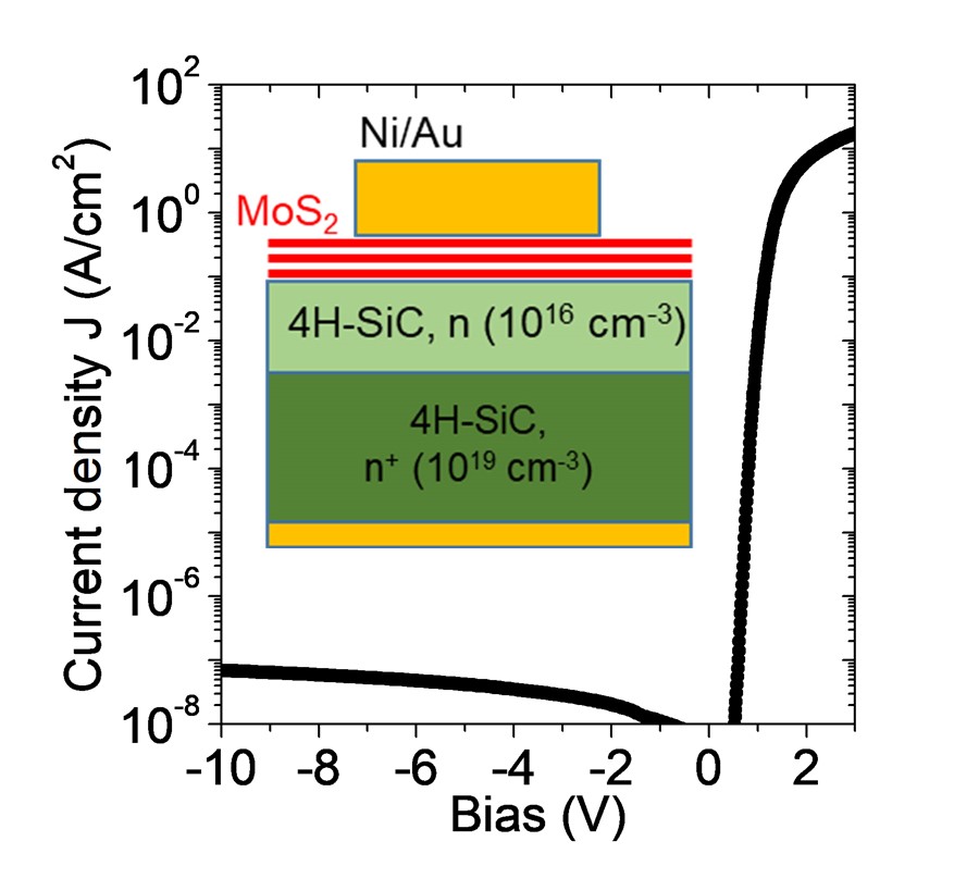
Current density versus bias characteristic of a MoS2/4H-SiC heterojunction diode, showing excellent rectification behaviour. Image adapted from Ref.[3]. Copyright Wiley, 2023.
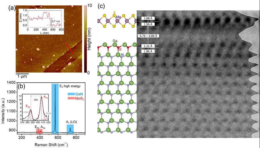
(a) AFM, (b) Micro-Raman, and atomic resolution STEM characterization of monolayer MoS2 films grown on GaN. Image adapted from Ref.[2]. Copyright Elsevier, 2023.
Author bio

Letizia Diamante
Science Writer and Coordinator of the 'Diversity in Graphene' initiative.