2D-EPL: Modules for the industry
The 2D Experimental Pilot Line (2D-EPL) project’s Modules for the Industry Work Package will develop dedicated fabrication processes for sensing, electronics and photonics applications, and prepare and perform multi-project wafer (MPW) runs which will be offered to external clients. The MPW runs will fabricate graphene-based devices for external clients (companies, research centres and universities) based on their individual designs. This will enable us to test and validate the process technology developed in the 2D-EPL.
This year’s progress
In the past year, our work package has worked with the Wafer Scale Integration Work Package to apply the processes that they have developed to our upcoming MPW runs. Work has also been performed with the 2D Pilot Line and Management Work Packages to resolve the administrative and dissemination processes involved in launching the first MPW run.
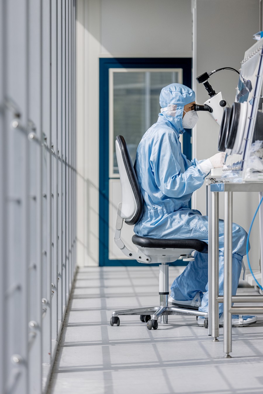
A scientist working on a chip housing in the AMO cleanroom. Credit: AMO
Collaboration
An important aspect of the 2D-EPL in general, and for our work package specifically, is the interaction with the Industrial Advisory Board, a group of individuals from influential European companies who provide input on the most relevant application areas for the 2D-EPL. This group is also instrumental in helping to promote the MPW runs amongst their networks.
What’s in store
In 2022 the first and second MPW run will launch focusing on sensor applications using graphene field effect devices. The chips from this MPW run could be used for a number of possible sensors: bio-sensors, light sensors, Hall-Sensors or chemical sensors. In photonics the applications are in sensing and telecom, and in electronics we are developing processes for novel transistor technologies based on 2D semiconductors. Completing the first MPW run will be our biggest challenge in the coming year. At this point it is unclear how many and what types of clients the project will receive.
Moving forward, the key challenge for our work package will be to properly address the needs of the MPW run clients and to maximise the impact of the 2D-EPL project. In total four or five MPW runs are planned and the lessons from one run will be used to improve subsequent runs.
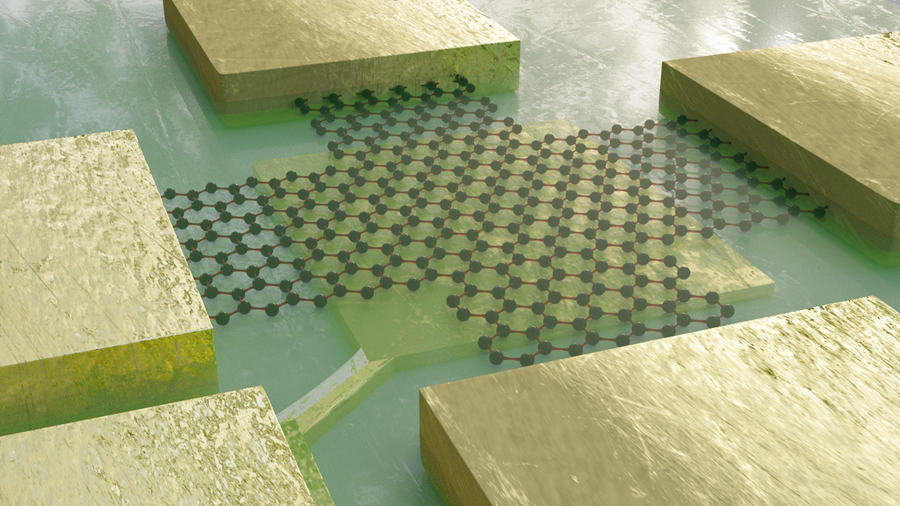
A sensor device schematic fabricated in the first multi-project wafer run. Credit: AMO