Pioneering 2D Materials for semiconductor industry
2D material transfer challenges on a wafer scale
We welcomed over 300 attendees to this workshop, hosted by the Graphene Flagship's 2D-EPL, which focused on the different steps that are encountered during the transfer of 2D materials on Si wafers, which secure access to the most advanced nanofabrication technology. The challenges linked to the delamination of high quality 2D materials grown on epitaxial templates as well as the subsequent steps for bonding the 2D materials to the target wafer were subject to an in depth dive.
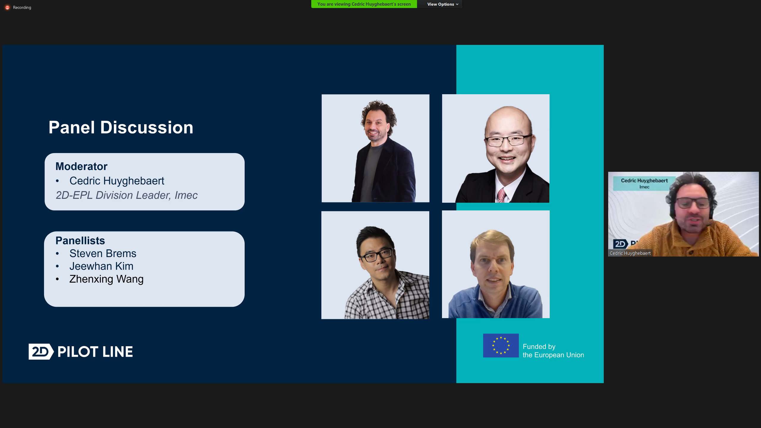
Keynote speakers & Panellists

Jeehwan Kim
Associate Professor

Cedric Huyghebaert
Research Manager Nano Applications Material Engineering
Steven Brems
Team lead ‘Material Transfer’
Zhenxing Wang
Group Leader, Graphene Electronics
Jeehwan Kim
Prof. Jeehwan Kim's group at MIT focuses on innovations in nanotechnology for next generation computing and electronics. Prof. Kim joined MIT in September 2015. Before joining MIT, he was a Research Staff Member at IBM T.J. Watson Research Center in Yorktown Heights, NY since 2008 right after his Ph.D. He worked on next generation CMOS and energy materials/devices at IBM. Prof. Kim is a recipient of 20 IBM high value invention achievement awards. In 2012, he was appointed a “Master Inventor” of IBM in recognition of his active intellectual property generation and commercialization of his research. After joining MIT, he continuously worked nanotechnology for advanced electronics/photonics. As its recognition, he received LAM Research foundation Award, IBM Faculty Award, DARPA Young Faculty Award, and DARPA Director’s Fellowship. He is an inventor of > 200 issued/pending US patents and an author of > 50 articles in peer-reviewed journals. He currently serves as Associate Editor of Science Advances, AAAS. He received his B.S. from Hongik University, his M.S. from Seoul National University, and his Ph.D. from UCLA, all of them in Materials Science.
Steven Brems
I received my MSc. degree in Applied Physics (cum laude) and my technical management degree in Economics in 2003 from the Technical University of Eindhoven. My PhD degree investigated magnetic interactions between antiferromagnetic and ferromagnetic layers and was obtained at the KuLeuven in 2007 and was funded by the research foundation Flanders (FWO). Next, I fulfilled several research functions at Imec. I was first involved in chemical/mechanical cleaning processes (spray and megasonics) to reduce particle contamination. I was involved in the growth and transfer of graphene to enable a CMOS compatible graphene integration. This challenge was later accompanied with the transfer of MX2 materials to facilitate the fabrication of the next generation transistor devices.
As team lead of Imec’s ‘Material transfer’ team, I am guiding the development of a CMOS compatible 2D transfer, but also following challenges related to Wafer-to-Wafer, (collective) Die-to-Wafer hybrid bonding and III/V material transfer approaches. Another important topic in which my team is involved relates to the fabrication and evaluation of the next generation pellicles based on carbon nanotubes. Such a pellicle needs to achieve a very high and uniform EUV transmission while being mechanically and chemically stable during prolonged high intensity EUV exposures. At the same time, I am involved in graphene EU flagship projects (e.g., 2D experimental pilot line and SH8) that aim to demonstrate a scalable 2D transfer and the latter project even aims to establish a small wavelength infrared camera for the automotive industry using a scalable 2D integration process.
Agenda
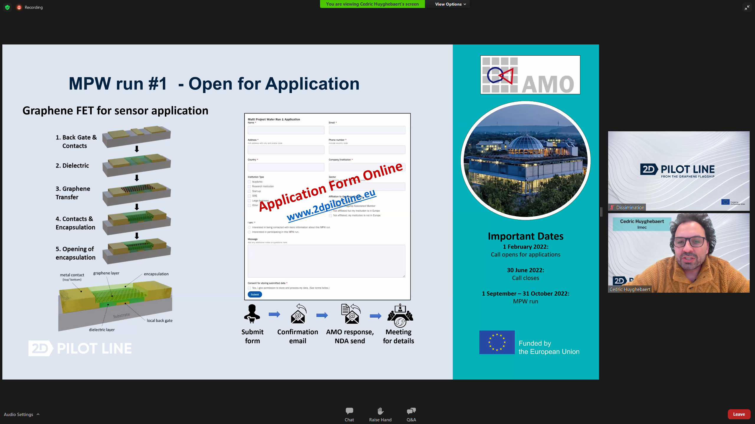
14:00 - 14:15 | Cedric Huyghebaert, imec
2D Experimental Pilot Line update. Announcing the call for applications to participate in the 2D-Experimental Pilot Line's first Multi-Project Wafer (MPW) run.
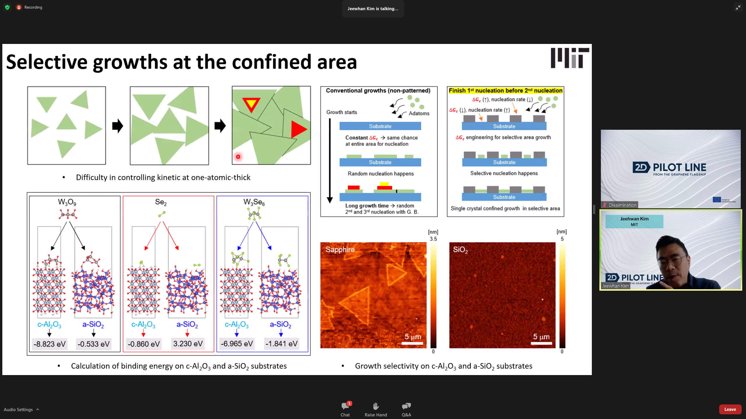
14:15 - 14:55 | Jeewhan Kim, MIT
Deterministic wafer-scale growth and transfer of single-domain 2D materials
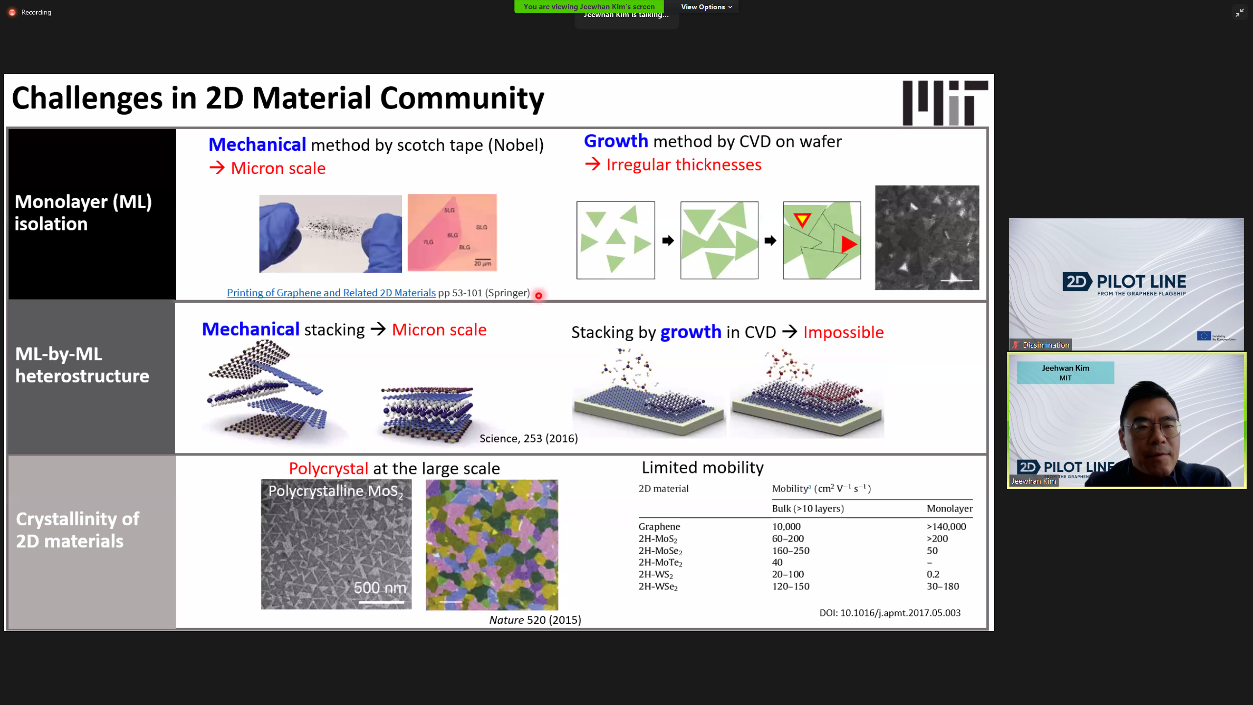
2D material-based devices have received great deal of attention as they can be easily stacked to obtain multifunctionality. With their ultrathin thicknesses, such multifunctioning devices become so flexible and conformal that they can be placed onto any 3D featured surfaces. However, 2D heterostructures are typically demonstrated as stacked flakes where single or few devices can be fabricated due to lack of strategies for layer-by-layer stacking of 2D materials at the wafer scale. While the growth technique could form wafer-scale 2D materials, it has been difficult to control monolayer-by-monolayer growths. In this talk, I will discuss about our unique strategy to isolate wafer-scale 2D materials into monolayers and stack them into a heterostructures by using a layer-resolved splitting (LRS) technique [1-2]. In addition, I will introduce our new technique to directly grow monolayer single-domain 2D materials at the wafer-scale and monolayer-by-monolayer growth of 2D heterostructures [3].
While 2D heterostructures promise interesting futuristic devices, the performance of 2D material-based devices is substantially inferior to that of conventional 3D semiconductor materials. However, 3D materials exist as their bulk form, thus it is challenging to stack them together for heterostructures. My group at MIT has recently invented a 2D materials-based layer transfer (2DLT) technique that can produce single-crystalline freestanding membranes from any compound materials with their excellent semiconducting performance [4-5]. I will also introduce my group’s 3D heterostructures by stacking various freestanding single-crystalline membranes to obtain new functionality [6].
References: [1] Science, 342, 833 (2013), [2] Science 362, 665 (2018), [3] unpublished, [4] Nature 544, 340 (2017), [5] Nature Materials 17, 999 (2018), [6] Nature, 578, 75 (2020)
14:55 - 15:25 | Steven Brems, imec
2D material transfer: The challenging route from LAB to FAB
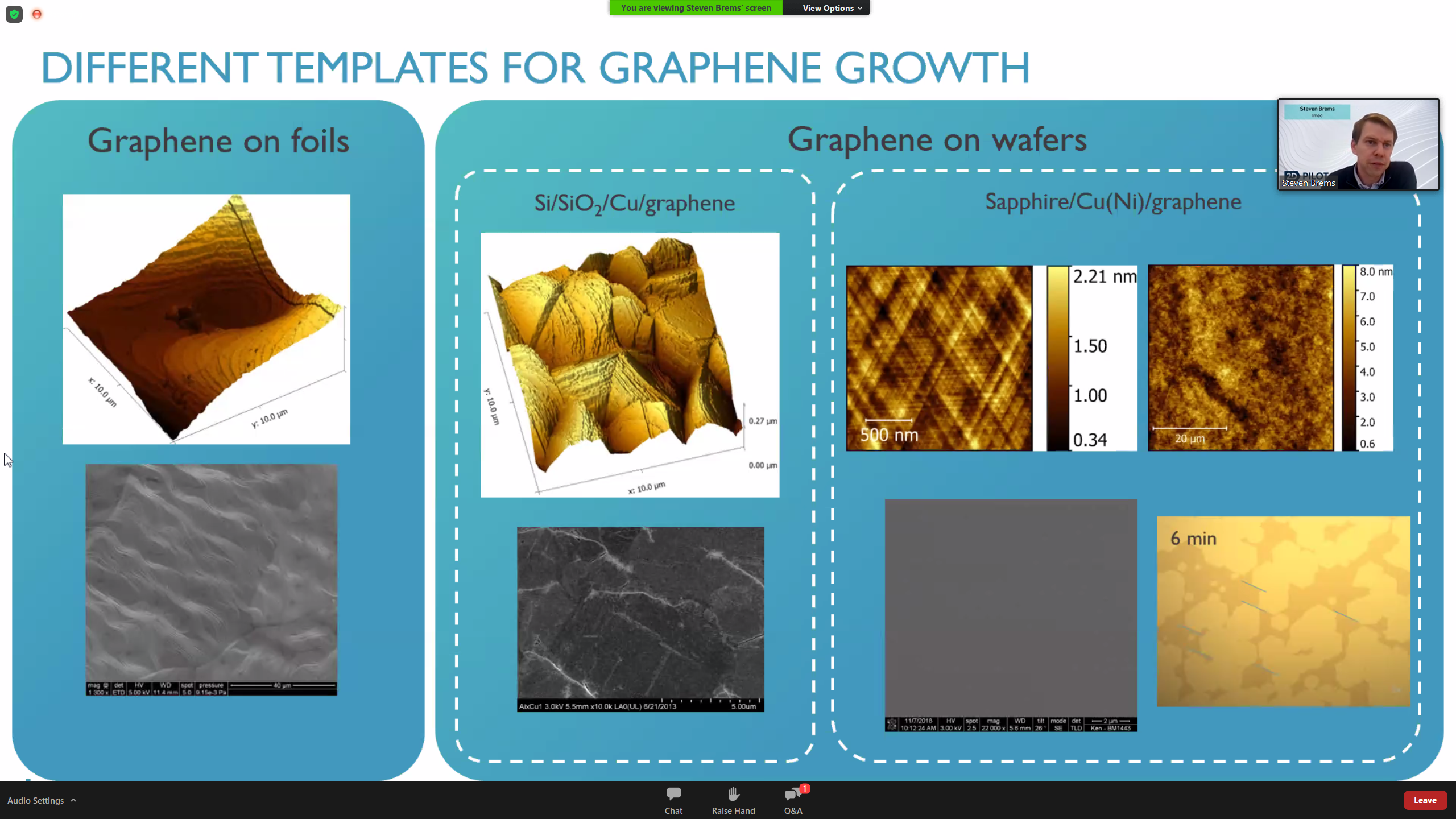
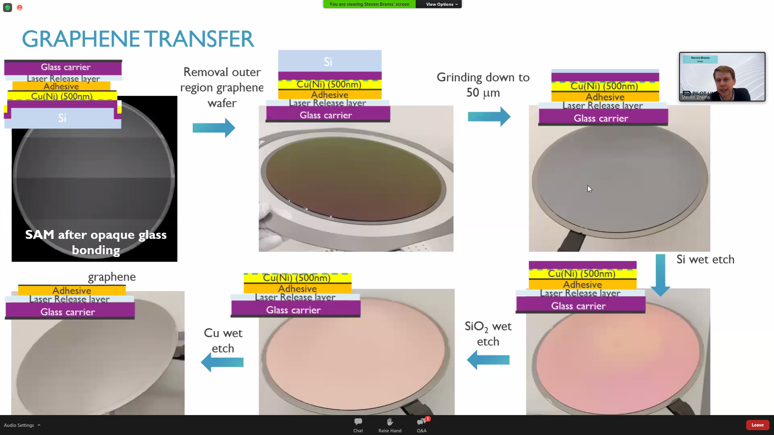
Despite the sizeable effort to synthesise two-dimensional (2D) materials and demonstrate devices with these layers, the commercial adoption of 2D layers in the semiconductor industry did not yet fully materialise. Several challenges need to be solved (e.g., high-quality 2D growth, dielectric growth on a passivated 2D surface, controlled interfaces...) to achieve this goal. Chemical Vapour Deposition (CVD) is the most mature and industry relevant synthesis technique to produce oriented growth of graphene, h-BN and MX2 (e.g. WS2, MoS2). Oriented 2D layers are typically grown at high temperatures (often well above 700°C), and regularly even using a catalytic layer to enable high-quality 2D growth (i.e., graphene and h-BN). A possible 2D material integration route relies on the transfer of these 2D materials from the growth substrate to the device wafer. This presentation focusses on the 2D material transfer challenges to achieve a CMOS compatible 2D transfer.
An industrial relevant transfer process is being developed for graphene and MX2 layers at Imec, relying on a rigid carrier combined with a laser release layer. A rigid carrier is likely one of the necessary requirements to enable the use of today’s bonding infrastructures, while maintaining strain control in these 2D layer during the different transfer steps. An overview of the challenges related to 2D material debonding from the growth substrate for both graphene and MX2 will be given. An understanding of the debonding mechanism will be shown, which often relies on water intercalation when the 2D material is directly de-bonded from the growth surface. To end, an alternative transfer process for graphene will be discussed, avoiding the need for a graphene peeling step directly from the growth surface. Alternative debonding methods might become more important to enable a 2D material adaptation by the industry.
15:25 - 15:55 | Panel Discussion
Our speakers will continue the discussion on transfer challenges. The panel will be open to your questions relating to the previous presentations or other related topics.
Moderator: Cedric Huyghebaert
15:55 - 16:00 | Closing thoughts