


New technique to 'clean' layered heterostructures improves device performance and paves the way to scalable production
Removing impurities between layered materials using heat and pressure increases charge carrier mobility and brings scalable methods closer to becoming a reality.
Graphene and related materials (GRMs) are like ingredients for a sandwich. You can stack them in any order and mutual angle and obtain so-called 'heterostructures'. Semiconductor-based heterostructures are key enablers for applications such as terahertz lasers and high-speed electronics, but current technology is limited in terms of materials combinations. GRMs provide a completely new platform for heterostructures, as different materials with very different properties can be carefully stacked, offering unprecedented flexibility in terms of possible combinations and engineering of specific functionalities on demand.
However, researchers find it challenging to make these 'sandwiched' heterostructures without introducing impurities between the layers. Now, a team led by Antonio Lombardo from Graphene Flagship partner the University of Cambridge, in collaboration with researchers from Graphene Flagship partner the University of Trento, and the National Institute for Materials Science, Japan, have devised a way to avoid this complication, and have been able to produce clean GRM heterostructures with better electronic properties.
To make these cleaner 'sandwiches', researchers first prepared the heterostructure following standard procedures, then applied heat and pressure to remove the impurities between the layers. Lead author Antonio Lombardo explains: "When you install a screen protector on your phone, you will probably get many bubbles across the surface. Something similar happens when we prepare heterostructures, when contaminants get trapped in the interface and aggregate in blisters. Much like when you remove the air bubbles on your screen by applying pressure with a hard-plastic card, we developed a technique that uses both heat and pressure to remove the impurities by pushing them away from the heterostructure. We remove contamination from all the interfaces simultaneously after the full structure is assembled, leaving an atomically clean interface over the entire surface of the sample much faster than any previous method."
Thanks to this innovative approach, researchers can obtain cleaner-than-ever graphene. "Our material has a room-temperature charge carrier mobility of about 180,000 cm2/Vs, significantly higher than any other material developed previously," explains Lombardo. "We also intentionally contaminated our samples before encapsulation, and after applying our cleaning method, the properties of the material are identical to originally clean samples, showing the effectiveness of the technique."
Moreover, Lombardo's team at Graphene Flagship Partner the University of Cambridge (UK), together with Graphene Flagship partners at ICFO (Spain), and the University of Palermo (Italy), together with colleagues from the National Institute for Materials Science in Japan, recently applied this cleaning technique to CVD graphene prepared by wet transfer. Wet transfer is a graphene manufacturing procedure that, although quick, cheap, and scalable, usually introduces a lot of contamination. Impurities usually come from the use of products such as etchants, polymers and solvents throughout the process. By combining encapsulation in hexagonal boron nitride with the newly developed cleaning method, researchers improved room temperature electron mobility up to 70,000 cm2/V·s in single-crystal graphene, and up to 30,000 cm2/V·s in polycrystalline films. All these figures are much higher than 10,000 cm2/V·s – the value that experts consider optimal towards realistic application of graphene in integrated (opto)electronics.
Marco Romagnoli, Graphene Flagship Work Package Leader for Wafer-Scale System Integration says that the work by Lombardo and colleagues "represents a major step forward and could lead to significantly improved electronics and (opto)electronics. This approach now needs to be implemented to enable effective wafer scale integration of graphene and related materials".
Frank Koppens, Graphene Flagship Work Package Leader for Photonics and Optoelectronics and co-author of one of the papers reported, says: "(Opto)electronic applications require uniform graphene of good mobility. This work paves the way to large-scale, high-quality graphene, even at wafer scale."
Andrea C. Ferrari, Graphene Flagship Science and Technology Officer and Chair of its Management Panel, adds: "One major goal of the Graphene Flagship is wafer-scale integrated photonics exploiting graphene and related materials. This work is a milestone since it shows how to optimize the simplest and most scalable transfer techniques to meet the requirements enabling devices based on graphene and related materials to beat the current state of the art in industry."
References
'High-mobility, wet-transferred graphene grown by chemical vapor deposition.' D. De Fazio, D.G. Purdie, A. Ott, P. Braeuninger-Weimen, T. Khodkov, S. Goossens, T. Tanhiguchi, K. Watanabe, P. Livreri, F.H.L. Koppens, S. Hofmann, I. Goykhman, A.C. Ferrari, A. Lombardo. ACS Nano 13, 8926 (2019).
'Cleaning interfaces in layered materials heterostructures.' D.G. Purdie, N.M. Pugno, T. Taniguchi, K. Watanabe, A.C. Ferrari, A. Lombardo. Nature Communications 9, 5387 (2018).
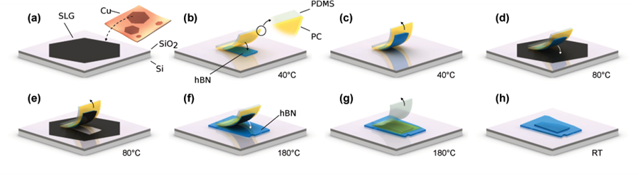
Schematic diagram of the sandwich structures. Credit: ACS (2019)
Author bio

Graphene Flagship
Bringing together 118 academic and industrial partners in 12 research and innovation projects and 1 coordination and support project, the Graphene Flagship initiative will continue to advance Europe’s strategic autonomy in technologies that rely on graphene and other 2D materials. The initiative, which builds on the previous 10-years of the Graphene Flagship, is funded by the European Commission’s Horizon Europe research and innovation programme. The 2D-Experimental Pilot Line, addressing the challenges of upscaling 2D material production processes for the semiconductor industry, is another key component of the Graphene Flagship eco-system.