Spintronics
Developing novel spin device paradigms
The Spintronics Work Package has achieved an unquestionable international leadership in discovering new spin transport phenomena by combining different types of layered materials into van der Waals heterostructures, fabricating some of the most complex device architectures and establishing state-of-the-art knowledge and prediction of novel spin device paradigms.
The last 10 years
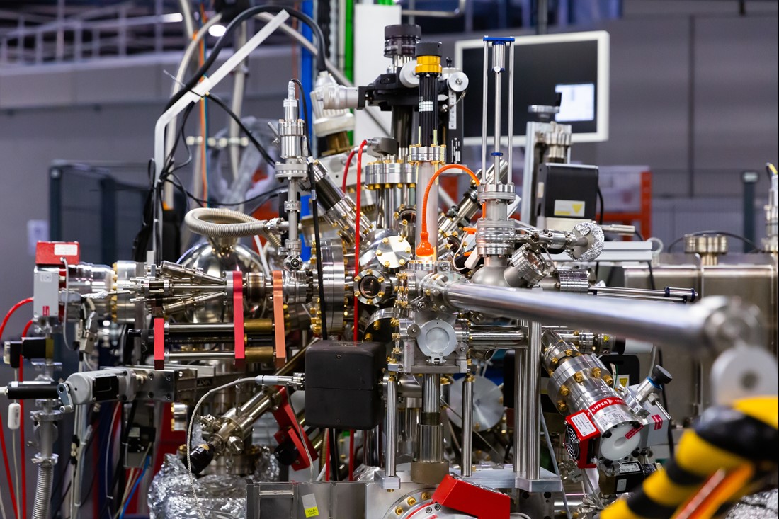
In its initial phase, the Spintronics Work Package addressed key questions, such as the origin of spin relaxation mechanisms in graphene. Thanks to studies marrying theoretical simulations and advanced device fabrication, the Work Package investigated spin transport efficiency limitations in CVD-grown graphene materials and mitigated them to achieve the upper limit of spin diffusion length at room temperature. In its second phase, the Work Package monitored proximity effects between graphene and other two-dimensional materials, making graphene “magnetic” or spin-dependent responsive. Major scientific breakthroughs were achieved, such as room-temperature spin current generation and demonstration of electric field control. Finally, the Work Package has pushed the frontier of knowledge by integrating layered materials into advanced non-volatile memory technologies: the first demonstration of large-scale integration of graphene into a magnetoresistive random-access memory (MRAM) stack.
The increased relevance of our collaborations with several companies, such as Singulus Technologies and Graphenea, and reasearch institute imec, have played a key role in exploring the co-integration of layered materials with conventional magnetic materials used in commercial memory technologies. The roadmap established by this Work Package in collaboration with companies like Samsung, Global Foundries and THALES highlights the need for further efforts, funding and consolidated support to keep transferring knowledge towards real applications.
This year’s progress
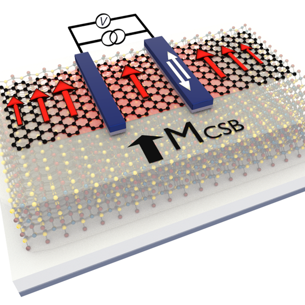
In 2022 the Spintronics Work Package developed several spintronic devices that were published in top level journals. For example, researchers worked on spin-valves that avoid conventional, air-sensitive magnetic contacts. The new device uses the spin properties of electrons in graphene to create a spin signal via the interaction of graphene with an antiferromagnetic material called chromium sulphide bromide. Using graphene for both the generation and transport of the spin signal helped to avoid a common problem in spintronics, that is "conductivity mismatch" which is a difference in electrical resistance between different parts of the device.
New inverted spin-valve devices made from CVD-grown bilayer graphene and hexagonal boron nitride (hBN) were also developed and performed more than twice as well as the best bilayer graphene spin valves at room temperature. It showed spin lifetimes of up to 5.8 ns, a spin diffusion length of up to 26 µm at room temperature and high charge carrier mobility.
A Perspective article in Nature was also published to highlight the prospects and challenges of non-volatile spintronic memories.

Stephan Roche, Work Package Leader
The Spintronics Work Package has established Europe as a global leader in spintronics based on layered materials and opened the road towards further developments for the next ten years.”
Work Package Leader
References
H Yang, H. et al. Nature, 2022, DOI: 10.1038/s41586-022-04768-0
AA Kaverzin, AA. et al. 2d Mater. 2022, DOI: 10.1088/2053-1583/ac7881
Bisswanger, T. et al. Nano Lett. 2022, DOI: 10.1021/acs.nanolett.2c01119
Latest Articles

Spotlight: Developing new memory devices with Marie-Blandine Martin
2D materials for a major leap forward in non-volatile memory technologies
Graphene Flagship researchers at the Catalan Institute of Nanoscience and Nanotechnology (ICN2), Barcelona, have led the publication of Nature review that roadmaps the possibilities of 2D materials in spin-based memory technologies.

Hall effect measurements in variable environments
Graphene Flagship parnter NPL just launched a service to measure the electrical transport properties of materials and devices, including sheet resistance, resistivity, carrier type, density, and mobility.
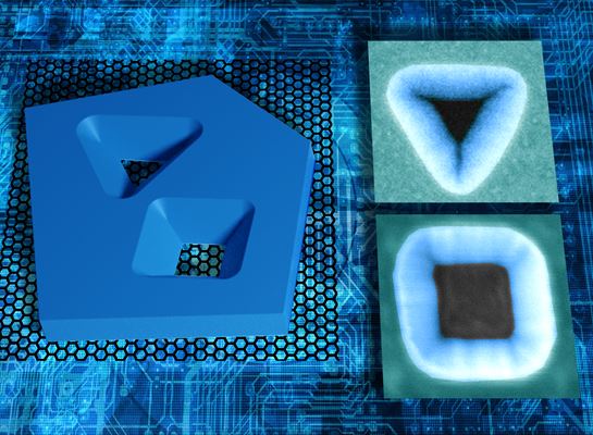
Ultrasharp patterning of layered materials
Patterning small and sharp geometries for the quantum technologies of the future

Graphene spintronics paves way to new computing technologies
Meet the team that explores the frontier of graphene and layered materials for memory, processing and more
Towards ultra-compact spin-logic circuitry with magnetic graphene
Spin polarisation has been introduced to graphene without a ferromagnet for the first time.